What EDA needs to change for 2020 success?
Dr. Olivier Coudert
What EDA needs to change for 2020 success
Dr. Olivier Coudert
![]()
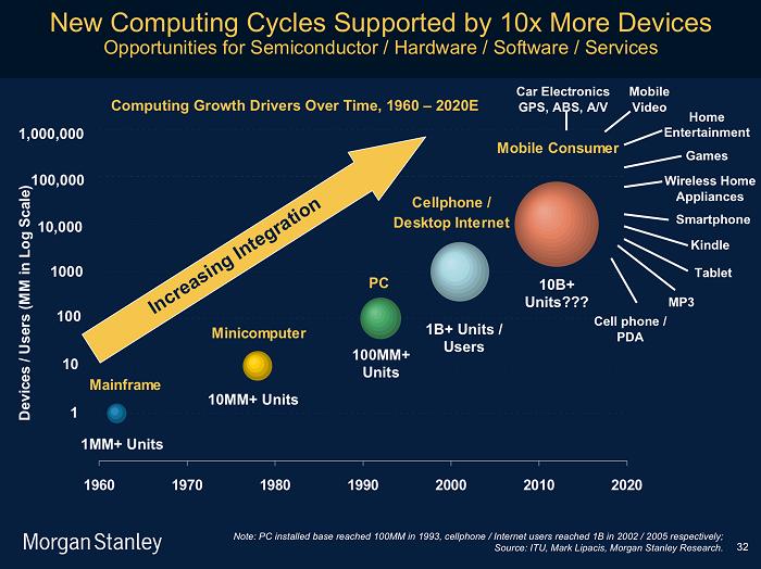
EDA is facing three trends. The first one is well know: the continuously rising cost of IC designs, about $50M for today’s 45nm node. The second trend is that the fastest growing part of the design cost is software –from half to 2/3rds of the overall cost. The third trend is an increasingly fragmented consumer market: the number of end products goes into the 10’s of billions, but these products are declined in many more different kinds, which means that most of them are shipping in smaller individual volumes.
 Source: Morgan Stanley, Economy + Internet Trends, Web 2.0 Summit, San Francisco, Oct 2009.
This is bad news for EDA as we know it: the rising cost of design can no longer be justified if the number of units does not grow fast enough (a $50M chip starts to make sense only if it is produced for 250M units and more). Also EDA has been slow to climb up the food chain and proposes solutions for software design, which dominates the overall chip design cost.
Rising IC design cost and smaller number of units is the call for FPGA to growth even faster. Mobile applications require FPGA to do much better in terms of power consumption, but this is a hot topic (no pun intended) drawing a lot of attention and investment, and some competitive solution will emerge in the next few years. So EDA, which makes its bread and butter on IC design, should better re-align its growth strategy on software, embedded systems, HW/SW co-design, and verification. Else EDA will continue to shrink to only service the few that can still afford chip design.
The end product, as a SoC, is a puzzle where the designer mostly assembles existing cores and IPs, and decides of the tradeoff between the software and hardware parts, based on flexibility and cost factors.
I see two strong needs that EDA could build its growth on. One is functional validation of the whole system –software plus hardware. EDA has started to Dr. Olivier Coudert address the issue, even though it is still short of proposing a scalable and automated environment. To functional validation, I would also add functional flexibility: how much of the behavior can be upgraded thanks to the software part? The other need is a design navigator that would estimate the speed, area, power consumption, and cost of a SoC by exploring alternatives between cores (ARM, MIPS, etc), IPs, FPGA, and software.
Last but not least, the eternal question of an EDA serving a $250B semiconductor industry, but making less than $5B. The time-based license model has only served the interests of the semiconductor companies, to the expenses of R&D investment in EDA. Claiming a lack of innovation in the EDA industry is sometimes fair, but EDA should also innovate in business solutions instead of cannibalizing itself by cutting costs to only survive another quarter. The semiconductor industry needs a healthy EDA if it wants to address the system-level design challenges of the next 10 years. Unless, of course, a new player coming from the software world with the experience of scalable systems signs the death of the EDA industry as we know it.
Dr. Olivier Coudert has 20 years experience in software architecture and EDA product development, including 10 years in research. He received his PhD in Computer Sciences from Ecole nationale supérieure des Télécommunications, Paris , France , in 1991. He has published 50+ papers and book chapters, and he holds several patents on combinatorial optimization and physical synthesis. He is a recognized expert in the fields of formal verification, logic synthesis, low power, and physical synthesis. He led the development of several EDA products, including 3 from scratch in a startup environment. You can follow Olivier on Twitter, meet him on LinkedIn, or read his blog.


