• אודות
  • כנסים ואירועים
  • צור קשר
  • הצטרפות לניוזלטר
  • TapeOut Magazine
  • ChipEx
  • סיליקון קלאב
  • Jobs
מבית
EN
Tech News, Magazine & Review WordPress Theme 2017
  • עיקר החדשות
    ין"ר TSMC ד"ר מוריס צ'אנג באירוע בשנחאי, 2007, איור: depositphotos.com

    כך הפכה TSMC למפעל השבבים המהימן ביותר

    תחזית שוק השבבים. אילוסטרציה: depositphotos.com

    תחזית ל־2026: תעשיית השבבים צומחת בזכות AI ורכב, אך נשארת תנודתית

    מיזוג נקספריה-מובי. צילום יחצ

    סין דורשת מהולנד לבטל את הצו נגד נקספריה: “התערבות מנהלית לא ראויה”

    תעשיית השבבים ואתגרי שרשרת האספקה. האיור הוכן באמצעות תוכנת הבינה המלאכותית DALEE

    ארה"ב השיקה את Pax Silica: קואליציה בת שבע מדינות לשרשרת האספקה בעידן ה-AI. ישראל בפנים!

    עסקת רכישת חטיבת הADAS של ZF בידי הרמן. צילום יחצ

    HARMAN רוכשת את פעילות ה-ADAS (מערכות סיוע לנהג) של ZF

    לי ג׳אה־יונג, יו״ר סמסונג אלקטרוניקס. צילום יחצ

    יו״ר סמסונג סייר באתרי השבבים בקוריאה, על רקע שיפור בביצועי חטיבת ה־DS

  • בישראל
    אוניברסיטת תל אביב. אילוסטרציה: depositphotos.com

    מחקר של אוניברסיטת סטנפורד קובע: לימודים באוניברסיטת תל אביב מגדילים ב־260% את הסיכוי להפוך למייסדי יוניקורן

    מיחשוב קוונטי. אילוסטרציה: depositphotos.com

    ויו־ביקס ו-Quantum X Labs הגישו בקשת פטנט זמנית לשיטה קוונטית לניתוח ניסויים קליניים

    InnovizTwo. צילום יחצ

    Innoviz חשפה את InnovizThree: חיישן LiDAR קטן וזול יותר המותקן מאחורי השמשה

    דרור בין מנכל רשות החדשנות. קרדיט חנה טייב

    רשות החדשנות משקיעה 40 מיליון שקלים בהקמה והפעלה של 5 אתרי הרצה לסטרטאפים לפיילוטים בתנאי אמת

    גארי גולמבו, מנכ״ל MosaIC, שתייצג בישראל את SignOff Semiconductors. (צילום: באדיבות החברה)

    SignOff Semiconductors הודיעה על פתיחת פעילות מכירות בישראל בשיתוף MosaIC

    לוגו סינופסיס. צילום יחצ

    הפיטורים בסינופסיס הגיעו גם לישראל. לאחר רכישת Ansys צפויה לפטר בין 20 ל-25 עובדים! חלקם כבר פוטרו

  • מדורים
    • אוטומוטיב
    • בינה מלאכותית (AI/ML)
    • בטחון, תעופה וחלל
    • ‫טכנולוגיות ירוקות‬
    • ‫יצור (‪(FABs‬‬
    • ‫צב"ד‬
    • ‫שבבים‬
    • ‫רכיבים‬ (IOT)
    • ‫תוכנות משובצות‬
    • ‫תכנון אלק' (‪(EDA‬‬
    • תקשורת מהירה
    • ‫‪FPGA‬‬
    • ‫ ‪וזכרונות IPs‬‬
  • מאמרים ומחקרים
  • צ'יפסים
  • Chiportal Index
    • Search By Category
    • Search By ABC
No Result
View All Result
Chiportal
No Result
View All Result

בית דפי האתר ושונות מוצרים חדשים Advantest Launches New Die-Level Handling System Enabling KGD Test Strategy Required for Memory, Large High-Power, and Advanced 2.5D and 3D Semiconductors

Advantest Launches New Die-Level Handling System Enabling KGD Test Strategy Required for Memory, Large High-Power, and Advanced 2.5D and 3D Semiconductors

מאת Webmaster
02 יוני 2016
in מוצרים חדשים
HA1000-0085910
Share on FacebookShare on TwitterLinkedinWhastsapp

New HA1000 System Tests ICs for High-Growth Applications Including Mobile Electronics and High-Performance Networking


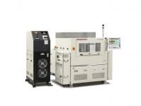
Munich, Germany, 01.06.2016 – Leading semiconductor test equipment supplier Advantest Corporation (TSE: 6857) has introduced its HA1000 die-level handler, a cost-efficient test solution for determining known good dies (KGD) prior to IC packaging.


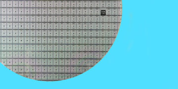
Economics is a driving factor in die-level testing. Determining a semiconductor device’s viability prior to packaging or building memory stacks is critical to avoiding rework, achieving high yields and lowering costs. Performing pre-assembly testing of singulated devices provides a new level of visibility into the quality of the device prior to committing additional devices and expensive packages to an assembly which could potentially have to be scrapped because of undetected problems. Advantest’s new die level handler allows full device testing to be performed before assembly, providing time-critical information that today is typically only available at final test.


“Testing and debugging today’s 2.5D, 3D and fine-pitch chip-scale-package devices require a KGD approach capable of testing the ICs while they are still in die form,” said Zoë Conroy, manager, Silicon Test and Product Engineering, Technology and Quality, Supply Chain Operations of Cisco Corporation. “Using the HA1000 to do KGD testing has enabled a faster time-to-market, lowering the overall product cost.”


Koichi Tsukui, senior vice president at Advantest Corporation commented, “We have leveraged knowledge stemming from decades of experience in device handling and thermal control technology to develop this new class of die-level-handlers. Our customers can now precisely position and probe singulated devices after they have been bumped, thinned and sawed. They will realize improved yields at final assembly, and that is an important achievement.”


Advantest’s HA1000 is designed to handle a wide variety of devices from large high-power server/GPU type devices to small system-on-chips (SoCs) and memory devices/stacks, such as HBM2. The die-level-handler can handle thick parts and thin parts as well as stacks of 3D devices and partially or fully assembled 2.5D integrations. In addition, the HA1000 is ideal to probe fine-pitch pads, bumps, microbumps and pillars. Future applications of the system may also include the probing of Through-Silicon-Vias (TSVs).


The handler employs a precision vision alignment system capable of precisely positioning probe points to the finest pitch in use today. While properly positioning the chuck under the probes, the system can also adjust the planarity to match with the device surface to insure a solid device connection.


An active thermal control (ATC) system enables the HA1000 to adjust on the fly to temperature fluctuations at the die’s surface over a very broad dynamic range of -40˚ C to 125˚ C. The temperature of the thermal head quickly responds using a hot-cold fluid mix. Thanks to low thermal resistance and high thermal capacity the system can handle high power devices with a thermal responsiveness which is often better than is possible in a packaged environment. This allows manufactures to test parts at higher power levels and/or tighter margins which can improve yields while reducing scrap.

.Production units of the new HA1000system have already begun shipping


About Advantest

A world-class technology company, Advantest is a leading producer of automatic test equipment (ATE) for the semiconductor industry and a premier manufacturer of measuring instruments used in the design and production of electronic instruments and systems. Its leading-edge systems and products are integrated into the most advanced semiconductor production lines in the world. The company also focuses on R&D for emerging markets that benefit from advancements in nanotech and terahertz technologies, and has introduced multi-vision metrology scanning electron microscopes essential to photomask manufacturing, as well as a groundbreaking 3D imaging and analysis tool. Founded in Tokyo in 1954, Advantest established its first subsidiary in 1982, in the USA, and now has subsidiaries worldwide. More information is available at www.advantest.de .


For further information please contact:

Corporate Communications
Email: info@eu.advantest.com

Webmaster

Webmaster

נוספים מאמרים

PCB

כיצד ניתן למנוע שגיאות תכנון סכימטיות באמצעות האימות האוטומטי של סימנס

מוצרים חדשים

Mentor Graphics Announces Broad Embedded Product Portfolio Coverage for Xilinx Zyng UltraScale+MPSoC Platform

מוצרים חדשים

Samsung DFM and Mentor Calibre Pattern Matchin

מוצרים חדשים

Mentor Graphics Announces Xpedition System Designer for Comprehensive Multi-board Systems Development

Next Post

Samsung DFM and Mentor Calibre Pattern Matchin

כתיבת תגובה לבטל

האימייל לא יוצג באתר. שדות החובה מסומנים *

  • הידיעות הנקראות ביותר
  • מאמרים פופולאריים

הידיעות הנקראות ביותר

  • הפיטורים בסינופסיס הגיעו גם לישראל. לאחר רכישת Ansys…
  • SignOff Semiconductors הודיעה על פתיחת פעילות מכירות…
  • אב־טיפוס EUV סיני בשֶׁנְגֶ’ן מאותת על פריצת דרך, אבל…
  • תחזית ל־2026: תעשיית השבבים צומחת בזכות AI ורכב, אך…
  • אינטל משיקה את AI Playground 3.0: מהפכה בנגישות ה-AI…

מאמרים פופולאריים

  • לקרב את המחשבים ליעילות האנרגטית של המוח
  • מדענים צפו בהיפוך ספיני אלקטרון בתוך 140 טריליוניות השנייה
  • צוות מחקר אוסטרלי גילה מדוע למחשבים קוונטיים יש…

השותפים שלנו

לוגו TSMC
לוגו TSMC

לחצו למשרות פנויות בהייטק

כנסים ואירועים

כנסים ואירועים

כנס ChipEx2026 יערך ב-12-13 במאי, 2026. הכנס מיועד לכל העוסקים בתעשיית הסמיקונדקטור  כולל מהנדסים, מומחים מקצועיים ובכירים.

ChipEx2026 will be held on May 12-13, 2026. The conference is intended for everyone involved in the semiconductor industry, including engineers, professional experts, and senior executives.

לחץ לפרטים

הרשמה לניוזלטר של ChiPortal

הצטרפו לרשימת הדיוור שלנו


    • פרסם אצלנו
    • עיקר החדשות
    • הצטרפות לניוזלטר
    • בישראל
    • צור קשר
    • צ'יפסים
    • Chiportal Index
    • TapeOut Magazine
    • אודות
    • מאמרים ומחקרים
    • תנאי שימוש
    • כנסים
    • אוטומוטיב
    • בינה מלאכותית
    • בטחון, תעופה וחלל
    • ‫טכנולוגיות ירוקות‬
    • ‫יצור (‪(FABs‬‬
    • ‫צב"ד‬
    • ‫רכיבים‬ (IOT)
    • ‫שבבים‬
    • ‫תוכנות משובצות‬
    • ‫תכנון אלק' (‪(EDA‬‬
    • ‫‪FPGA‬‬
    • ‫ ‪וזכרונות IPs‬‬

    השותפים שלנו

    כל הזכויות שמורות Chiportal (c) 2010 תנאי שימוש ומדיניות פרטיות

    דרונט דיגיטל - בניית אתרים, בניית אתרי וורדפרס, בניית אתרי סחר, חנות אינטרנטית, פיתוח אתרים

    No Result
    View All Result
    • עיקר החדשות
    • בישראל
    • מדורים
      • אוטומוטיב
      • בינה מלאכותית (AI/ML)
      • בטחון, תעופה וחלל
      • ‫טכנולוגיות ירוקות‬
      • ‫יצור (‪(FABs‬‬
      • ‫צב"ד‬
      • ‫שבבים‬
      • ‫רכיבים‬ (IoT)
      • ‫תוכנות משובצות‬
      • ‫תכנון אלק' (‪(EDA‬‬
      • ‫‪FPGA‬‬
      • ‫ ‪וזכרונות IPs‬‬
      • תקשורת מהירה
    • מאמרים ומחקרים
    • צ'יפסים
    • כנסים
    • Chiportal Index
      • אינדקס חברות – קטגוריות
      • אינדקס חברות A-Z
    • אודות
    • הצטרפות לניוזלטר
    • TapeOut Magazine
    • צור קשר
    • ChipEx
    • סיליקון קלאב

    כל הזכויות שמורות Chiportal (c) 2010 תנאי שימוש ומדיניות פרטיות

    דרונט דיגיטל - בניית אתרים, בניית אתרי וורדפרס, בניית אתרי סחר, חנות אינטרנטית, פיתוח אתרים

    דילוג לתוכן
    פתח סרגל נגישות כלי נגישות

    כלי נגישות

    • הגדל טקסטהגדל טקסט
    • הקטן טקסטהקטן טקסט
    • גווני אפורגווני אפור
    • ניגודיות גבוההניגודיות גבוהה
    • ניגודיות הפוכהניגודיות הפוכה
    • רקע בהיררקע בהיר
    • הדגשת קישוריםהדגשת קישורים
    • פונט קריאפונט קריא
    • איפוס איפוס